- Factory-Direct Pricing | No Middleman Markups
- Save 30%-My Sourcing
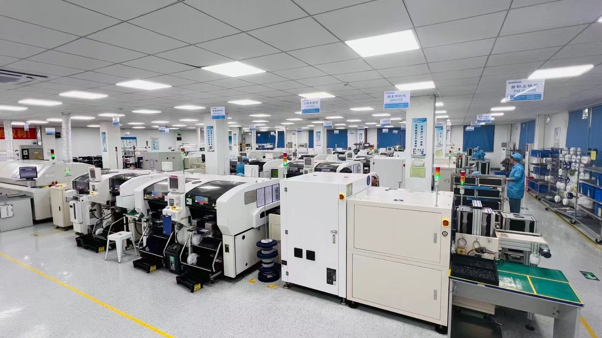 printed circuit board assembly manufacturer
Overpaying for printed circuit board assembly sourcing? Hire me to connect with PCB assembly factory-direct, cut out 30% costs! From Gerber files to delivery: DFX/DFM/QC support, optimizing layout, BOM parts sourcing, Let’s talk now!
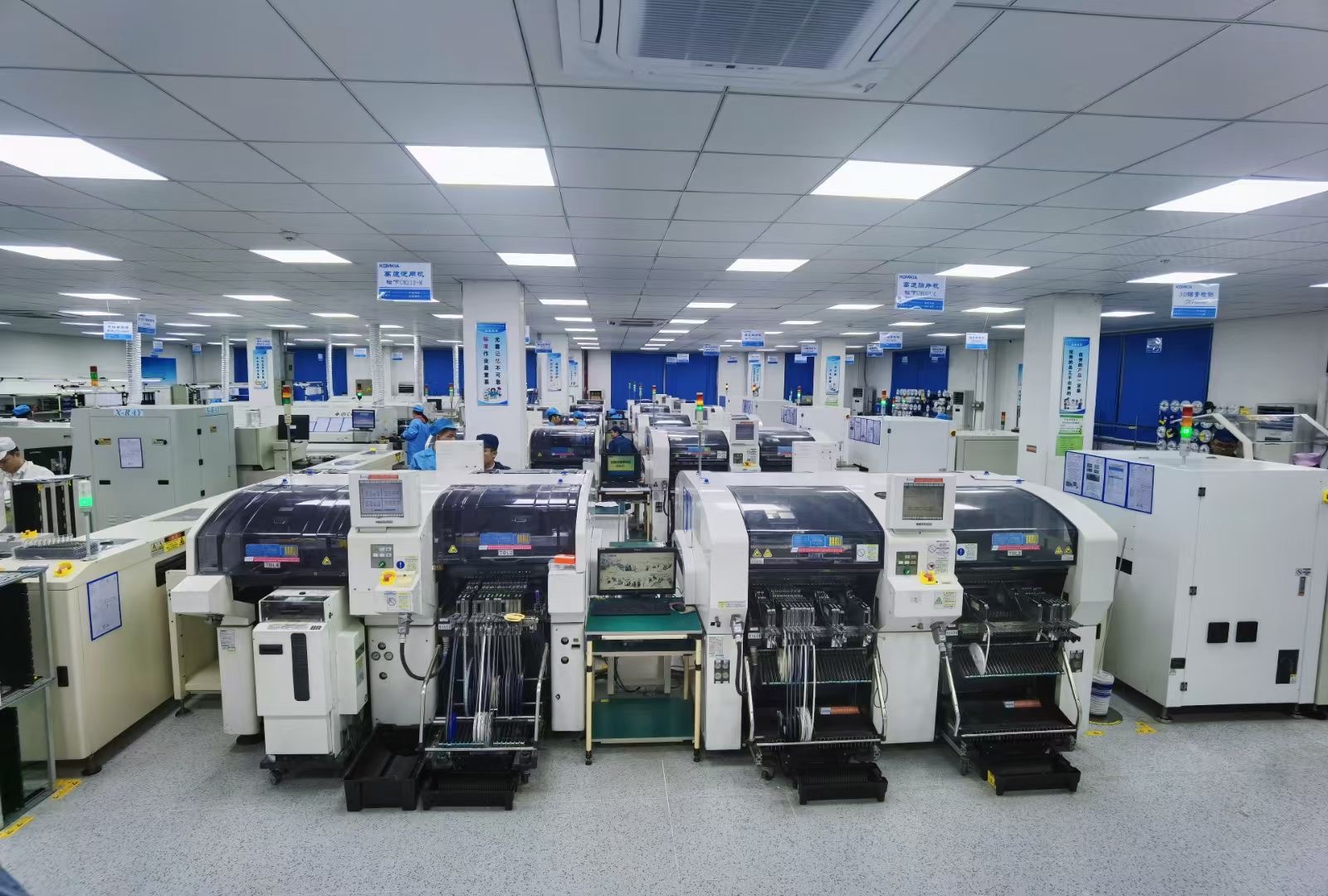
China dominates the global PCB assembly market, offering unparalleled expertise, cutting-edge technology, and cost efficiency. As a seasoned sourcing manager specializing in PCB assembly services, I streamline the process of securing high-quality, affordable printed circuit boards for clients worldwide. This article explores China’s PCB manufacturing ecosystem, detailing processes, industry applications, technology, quality assurance, cost advantages, and delivery reliability. Discover why partnering with a local expert like me ensures your project’s success.
China’s PCB manufacturing follows a meticulous 8-step workflow:
Design & Prototyping
Engineers use CAD software (e.g., Altium, Gerber, Eagle) to create schematics.
Prototypes are tested for functionality and compliance.
PCB Fabrication
Layering: Copper-clad laminates are etched to form conductive pathways.
Drilling: Precision machines create vias for component connections.
Component Sourcing
Procurement of MCU, ICs, resistors, capacitors, diode, transistor, Mos, and connectors, etc from vetted suppliers.
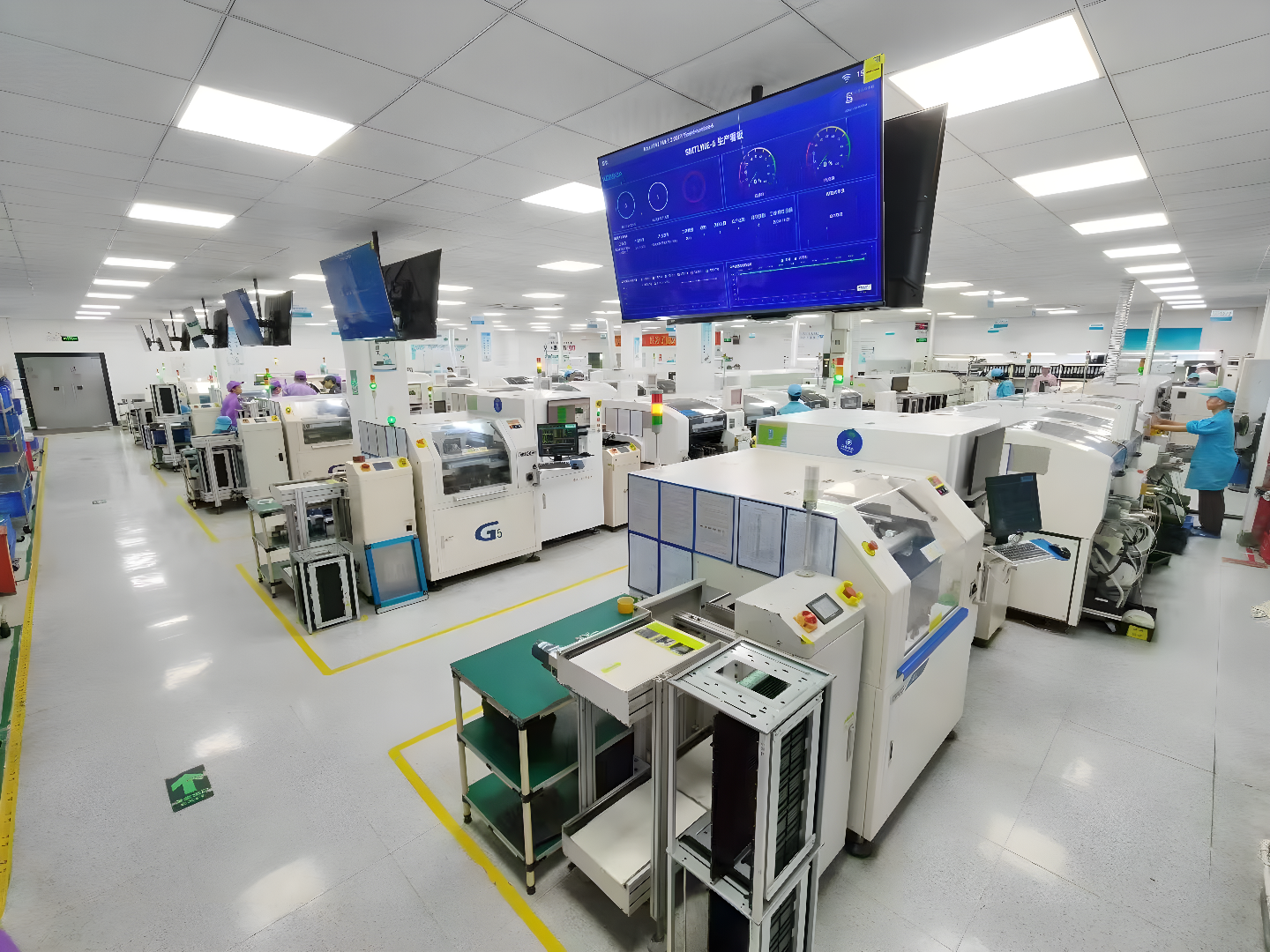
Surface Mount Technology (SMT)
Automated pick-and-place machines mount components at speeds up to 30,000 parts/hour.
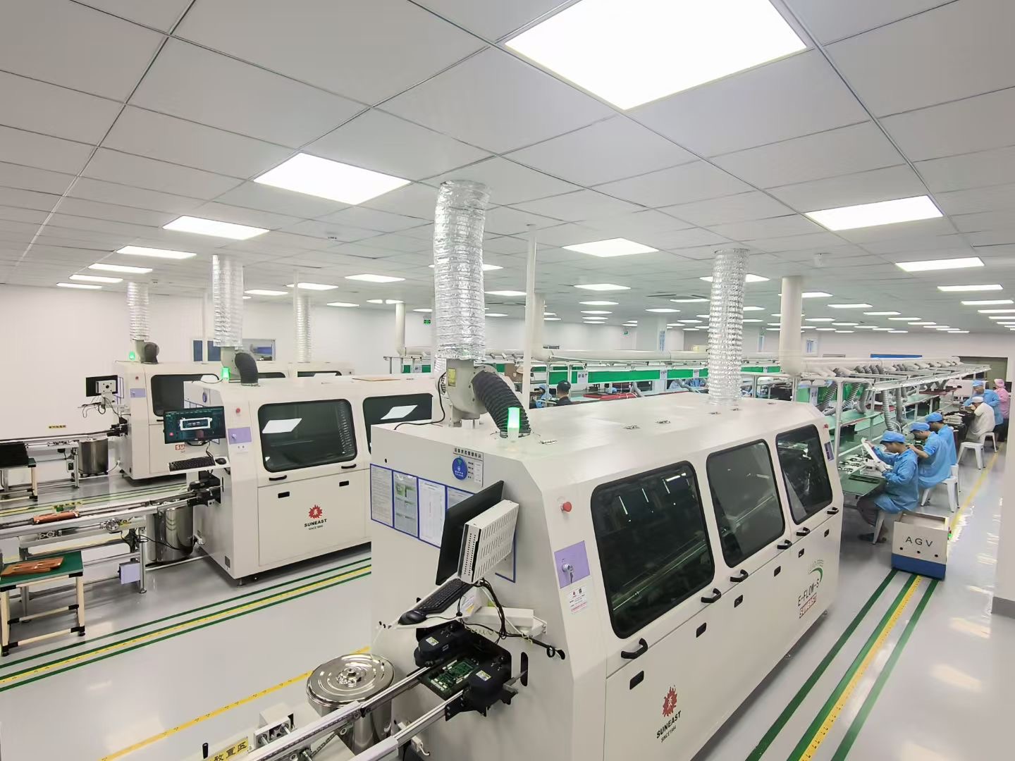
Through-Hole Assembly
Manual or wave soldering for larger components like transformers.
Inspection & Testing
AOI (Automated Optical Inspection) detects soldering defects.
X-ray Inspection verifies BGA and QFN connections.
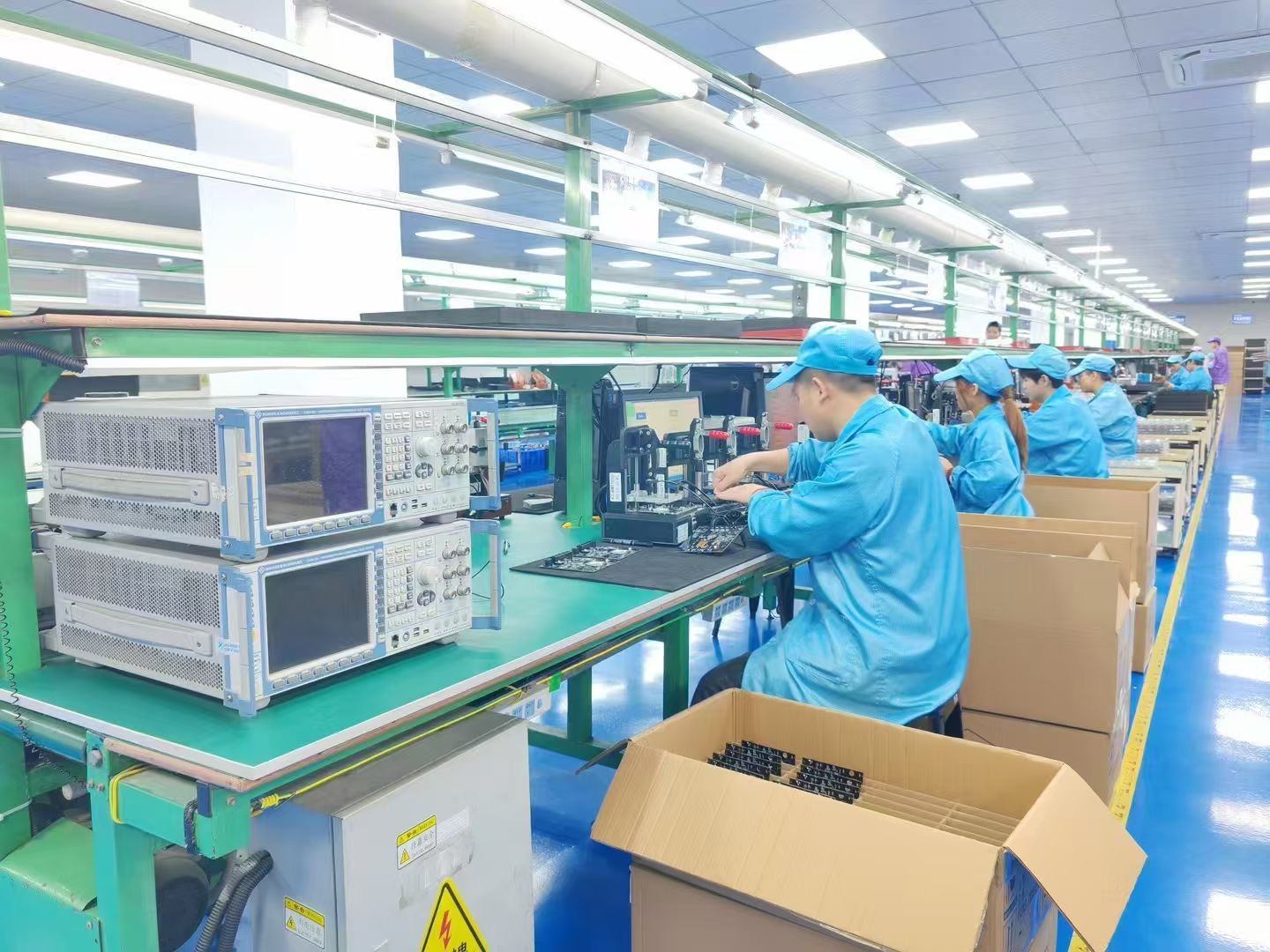
Functional testing simulates real-world performance.
Conformal Coating & Encapsulation
Protects boards from moisture, dust, and thermal stress.
Packaging & Logistics
Anti-static packaging and partnerships with DHL, FedEx ensure safe global delivery.
Consumer Electronics
Smartphones, wearables, and IoT devices demand high-density interconnect (HDI) PCBs.
Automotive
ADAS, EV battery management systems, and infotainment rely on robust, heat-resistant boards.
Medical Devices
MRI machines, pacemakers, and wearable monitors require ISO 13485-certified production.
Aerospace & Defense
MIL-spec rigid-flex PCBs for avionics and satellite communications.
Industrial Automation
Motor controllers, PLCs, and sensors built for harsh environments.
Telecommunications
5G infrastructure and RF modules using high-frequency materials like Rogers 4350B.
IoT & Smart Home
Compact, low-power designs for connected devices.
Renewable Energy
Solar inverters and wind turbine controllers with high-voltage tolerance.
Chinese factories adhere to:
ISO 9001, ISO 14001, IATF 16949, ISO 13485 certifications.
IPC-A-610/600 standards for acceptability and reliability.
100% Batch Testing: Thermal cycling, burn-in tests, and impedance analysis.
Testing: 100% electrical testing, 3D SPI (Solder Paste Inspection).
Testing Protocols: Thermal cycling, shock/vibration tests, and HALT (Highly Accelerated Life Testing).
Traceability: Barcoding and ERP systems for full component lifecycle tracking.
Labor Costs: Skilled technicians at 30–50% lower rates than Western counterparts.
Economies of Scale: Bulk material purchasing reduces unit costs by 15–30%.
Vertical Integration: Local suppliers for raw materials (e.g., Hong Kong and Shenzhen’s component markets).
Just-in-Time (JIT): Kanban systems for low-volume, high-mix orders.
Sea/Air Freight Options: 5–7 days for air shipments; 20–30 days via sea.
Local Warehousing: Inventory management hubs in Shanghai/Shenzhen.
As your dedicated partner, I mitigate risks and optimize your supply chain by:
Supplier Vetting: Pre-Auditing factories for technical capability, manufacturing process, quality control system and compliance.
Quality Oversight: On-site inspections and third-party lab testing.
Logistics Coordination: Leveraging DDP (Delivered Duty Paid) incoterms to simplify shipping.
Local Expertise: 10+ years in Guangdong’s PCB hubs (Shenzhen, Dongguan and Hong Kong).
Cost Negotiation: Secure 10–25% savings via competitive bidding.
Risk Mitigation: Resolve supply chain disruptions (e.g., component shortages).
China’s PCB assembly industry combines innovation, scalability, and affordability. By hiring me as your sourcing manager, you gain a trusted ally who navigates language barriers, cultural nuances, and logistical hurdles—ensuring your project meets deadlines, budgets, and quality benchmarks.
Ready to Streamline Your PCB Sourcing?
Contact me today to discuss your requirements and get a free consultation and quote. Let’s transform your designs into high-quality, cost-effective products!
FAQ Section
Q1: How do you handle intellectual property (IP) protection in China?
A: We enforce NDAs and work with factories certified under China’s IP protection laws.
Q2: Can you support small-batch orders?
A: Yes! Many Chinese suppliers specialize in prototyping and low-volume production.
Q3: What’s the typical lead time for PCB assembly?
A: 2–5 days for SMT orders; 2–4 weeks for complex multilayer boards.
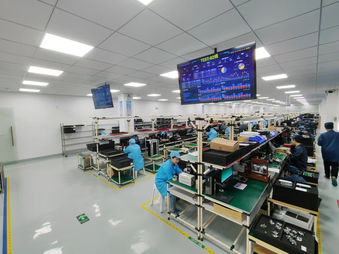
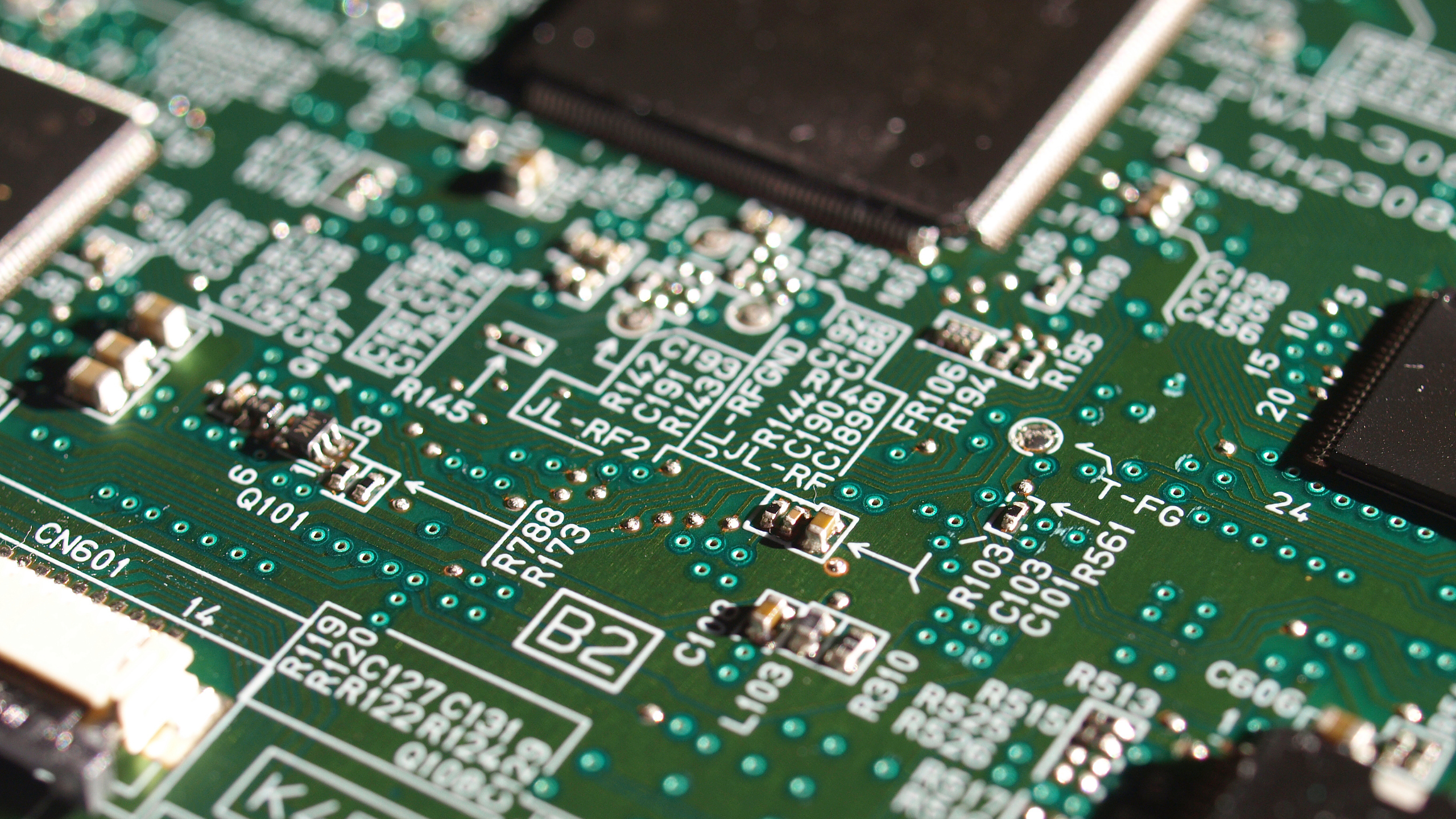
Automated Optical Inspection (AOI) testing is very common in the SMT industry and is suitable for all board production and PCB assembly. It is mainly used to judge the welding problems of components by the appearance characteristics of components. It can also be determined by checking the color and screen printing of the components on the IC, and whether the components on the circuit board are misaligned
FAI mainly is to do the first article PCBA through the integration of BOM table, coordinates and high-definition scanning of the first image automatic generation detection program, fast and accurate component detection, and automatically determine the result, generate the first article report. To achieve the purpose of improving production efficiency and capacity, while strengthening quality control.
DIP inspection is mainly inspect the bottom of the board, board surface, copper foil PCB circuit, through hole, etc., should have no cracks or cuts, no short circuit caused by bad cutting. The edge damage is acceptable within a certain length, more than the requirement is bad, bending degree is calculated based on the bending distance. Dip inspection ensure DIP processing compliance with quality standard.
X-RAY has strong penetration, and its perspective can show the thickness, shape and mass density distribution of the solder joint, which can fully reflect the welding quality of the solder joint, such as open circuit, short circuit, holes, bubbles inside the hole and insufficient tin and other quality problems.
ICT (In-circuit test) is contacted test technology, mainly used to mainly check out the failure problem includes bridge connection, false soldering, short circuit, open circuit, as well as the error such as component polarity and variety was mis-mounted, value overruns, etc.
FCT (Functional Circuit Test): PCBA power-up test, mainly including voltage, current, power, power factor, frequency, duty cycle, brightness and color, character recognition, sound recognition, temperature, pressure measurement, motion control, FLASH and EEPROM programing and other test items.
We offer our customers with free DFM checking: signal and mixing layer, power and grounding, drilling, soldermask and silkscreen analysis and checking, to ensure every detail is correct, and our engineers send engineering enquiries to our customers when they find any information that does not match with the original file or SMT process.
SPI is mainly used to check the quality of solder paste printing. It accurately measures and analyses the solder paste printed on the PCB by means of a high-precision camera and advanced image processing technology, including key parameters such as the height, volume, area, shape and position of the solder paste.
Steel surface tension standard in IPC electronic acceptance requirements contain reference indicators. The general use of steel mesh tension tester, placed at a distance of 15-20cm from the pitch, select 5-8 points, each square centimeter of tension is greater than 35 ~ 50 N. Ensure that the test results meet the specifications of the product.
+8619872870689
kinfomtech
No.1 Road East Hongfu, Dongcheng, Donguan, China.
+8619872870689
“From raw materials to retail-ready goods—we’re your all-in-one solution. Let’s optimize your chain!”